Thermal Signature of a Resistor
InfraMation 2015 Application Paper Submission
Jack Shue, Jay Brusse, Lyudmyla Panashchenko
National Aeronautics and Space Administration / Goddard Space Flight Center
ABSTRACT
Like all electronic parts the lowly resistor has its own set of failure modes and efforts are continuing to look for new and better ways to screen out parts that have built-in weaknesses. For the foil-based resistor some of the failure modes are holes in the conductive material, or excess materials that are not part of the design. While looking for a new screening method it was realized that both holes and excess materials can be detected by watching the part under test heat up. In the development of a screening test several classic problems were encountered. Among those encountered were in the following categories: 1. Moiré patterns, 2. Narcissus effects, 3. Emissivity, 4. Limits on Resolution.
The intention of this paper is to review what a resistor is, and why there are problems in making defect free parts, and then to explore some of the physical problems encountered in developing a test to weed out weak parts. All of this on a part size where 50 could fit on a penny with room to spare.
INTRODUCTION
The common resistor is arguably the simplest electronic part whose definition includes things like a heating element in an electric range. Depending on their usage, resistors can be big like those in an electric range, to some that can not be seen without the aid of a very good microscope. Recently some resistors that were intended to fly in space failed due to the limitations of the materials used. The failures were straight out of elementary physics in that the material was thin enough to become porous. In the quest for a better, more effective, screen for weeding out weak parts within the class of thin film resistors, it was questioned if a thermal camera would be a good way to determine if a resistor had defects. It was believed that the changes in the width of the metal trace would show up as a hot spot in the resistor, which the thermal camera could detect.
Previous test methods to detect flaws had included taking random samples from a set of parts and submitting the sample parts to destructive physical analysis (DPA), including stripping protective coatings from the top of the sample resistor and looking at them using high magnifications with a Scanning Electron Microscope (SEM). The use of DPA brings with it the age-old question of sample size, and the worry that the sample may not have the problem, and the parts to be used would still have the problem. The problem at hand was the breaking of the conductor internal to the resistor. It turns out that the thermal camera is a very good way to find the defects in question, and as a bonus, the temperature changes can be seen through the protective coating so parts do not need to be destroyed by a costly DPA. The experimentation and the lessons learned in the early testing will be the main focus of the paper, but as a teaser the end results are given at the beginning to show what can be accomplished. Following the final results will be a section on what a resistor is and how in building the part the physics leads to the problem, and that the problem can’t be avoided. Problems found during the experimentation are also unavoidable but once they are known there are ways to reduce the effects or at least understand them. Problems encountered and discussed are;
- Defects are small and a microscope is needed to see the small parts and even smaller defects.
- The design of the resistor uses many parallel traces and the design of the camera sensor also used parallel detectors. With the line width and the sensor widths nearing the same size the problem of Moiré patterns comes up and is addressed.
- The narcissus effect comes into play when a flat reflective surface is normal to the lens, and the inside of the camera is seen. This is a normal situation when using a thermal microscope and the data going into the surrounding air temperature correction factor becomes the temperature of the inside of the camera, and the internal temperature of the lens barrel.
- In the case of the resistor there were two very different emissivities of interest. The foil carrying the current is driving the heating, and the material below the foil is in effect the heatsink and should be cooler. When viewed using a single emissivity value, the foil appears to be the heatsink and the material below appears to be driving things.
- When using a microscope there is a limitation on how close one can get with a microscope. Included is a different perspective on what the limitation is on magnification, and why it is even more limited for thermal imaging.
THE RESULTS
NASA takes pride in what we do and we want our spacecraft to last a long time. Due to the nature of where the spacecraft work it is difficult if not impossible to repair what has been sent into orbit or into deep space. While things do sometimes fail, we try to do everything possible to make them work, and screening of parts is yet another way to find weak parts, as it is better to find them on the ground than to find them once they have been launched.
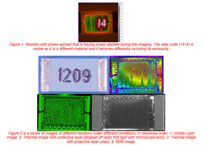
Not only was it possible to see parts of the resistor getting hotter it was also found that it was not necessary to remove any of the protective coating from the part. Figure 1 shows a sample part under test, and it shows a hot spot developing very quickly after power was applied to the part. In this case the part had all of its coating on, and the part’s date code shows due to the method of marking the part.
WHAT IS A RESISTOR AND WHY ARE THERE PROBLEMS IN MAKING A “SIMPLE” ELECTRONIC PART?
WHAT IS RESISTANCE?
The electrical resistance of an electrical conductor is the opposition to the passage of an electrical current through that conductor.
In mathematical form it is:
Where: R = Resistance (Ohms)
ρ = Resistivity of the material (Ohms – meters)
L = Length of the material; (meters)
A = Cross sectional area of the material (meters2)
And for the two materials used the constant ρ are:
ρ for Silver = 0.000,000,015,87 Ωm
ρ for Nichrome = 0.000,001 to 0.000,001,5 Ωm
Silver is a very good conductor and is used in electronics for its conductive properties. To build a 2000 Ω resistor out of silver with a cross section of 1 meter it would need to be 126,000,000,000 meters long. To give a perspective as to how long these would be, one would need a length of material that would go from the Earth to a point somewhere inside the orbit of Mercury.
Clearly, a resistor built with a good conductor (silver) would not make for a good economic resistor, as they would deplete the Earth of all of its resources for a single part. It is clear that a different material would be needed. Another material that is used in electronics is nichrome. With nichrome, ρ increases to 0.000,001 Ω to 0.000,001,5 Ω from silver’s 0.000,000,015. Clearly this is a factor of 100 better than silver, but it still makes for a bar of metal 1,700,000,000 to 2,000,000,000 meters long.
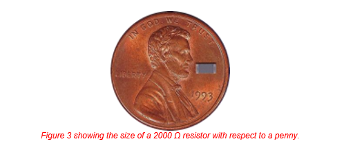
For the thin film resistor technology it is possible to roll out the metal into something much smaller than the 1 meter that this paper started with. It can be rolled down to a thickness of approximately 0.000002 meters thick, and for a piece of nichrome 0.000,002 meter by 0.000,002 meters a length of material 0.01 meters (1 centimeters) long would be needed. This would reduce the length of the resistor by 12 orders of magnitude, and now the length of the resistor becomes practical. Figure 3 gives a scale image of the resistor as it exists.
However appealing it is to make the resistor very small there are limits as to how small it can be made. The main problem is a limit on how small something can be reliably produced. In the case of thin film resistors there becomes a point where defects begin to overwhelm what the part can handle. Thin metals start to have holes and non-conducting materials imbedded in the material. At times this is attributed to a metal being porous and at other times the problem is as simple as a hole in the material. For the most part the manufacturing process must weed out or be able to perform within specification with the defects. The interaction of a defect and the resistive film is best described in the case of a hole in the material. A hole can be positioned in one of three ways. The first is the simplest and easiest to deal with; it is a hole that overlaps the spacing between the metal film. In this case there is no effect on the resistor. The second case is where the hole completely overlaps the trace. In this case the resistive path is broken and the part is seen to be defective immediately. The third case is somewhere in between the first two and allows the hole to be partially on the metal trace. In this case the metal is thinner than planned but still conductive. Electrically it can’t be seen but it now has a built in defect.
The reason for this is most easily seen by imagining the resistor as a series of lower value resistors. If a 2000Ω resistor was made up of 10000 0.2Ω resistors, one of the 10000 resistors could be replaced by a 2Ω resistor giving the total resistance of 2001.8Ω or a 0.09% difference which is within the tolerances given for the part. Even with what appears to be no change in the resistance of the part there will be a localized change in the resistor’s temperature however small it might be, as there is a 10 fold increase in the power dissipated in that area.
FIRST ROUND OF TESTING
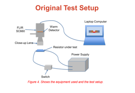
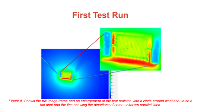
The first step was to see if the predicted temperature change could be seen and to use the temperature change to spot the defects and use it as a screen. The first part to be used had been stripped of its protective coatings and two defects had been spotted. Figures 4 and 5 show the original test configuration and the image resulting from the test.
ACCOMPLISHMENTS OF THE FIRST RUN WERE:
- Overall the resistor was getting hot with an increase of approximately 2 °C.
- Temperature rise at the one spot was maybe 2°C but we had hoped for and expected a 60°C rise.
- There were two defects on the resistor so there should be two hot spots. We barely saw maybe one
- There were unexpected diagonal stripes.
The results of the first trial run were less than stellar. It was possible to see the entire resistor heat up but there were plenty of explanations needed. The expected two defects seemed to be somewhere in the background noise. One location seemed promising to have a hot spot, but was this wishful thinking? When the math was done given the temperature delta of the different areas, and the size of the defect to that single pixel it was realized that the hot spot was about 1/25th of the pixel size. For such a small defect (and this was the big one) it was calculated that the hot spot temperature would have to be at about 60°C or higher to see anything in the image, and the second hot spot could not be imaged.
From what could be seen it was clear that there was something there, but to do what was wanted a better test setup was need, and the most important thing was a way of getting closer to the resistor and to see it with more detail. A thermal imaging microscope was needed.
THE PROBLEMS ENCOUNTERED.
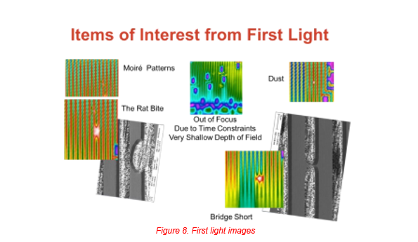
While looking back on the effort the problems encountered were all problems that could be foreseen, but what was seen and how the problems interacted is an interesting set of issues, and will form the rest of the paper with short descriptions of what those problems were.
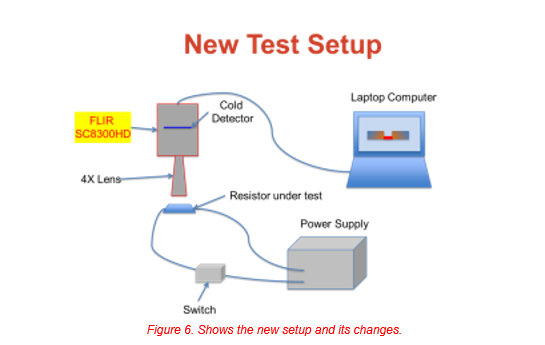
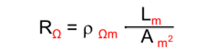
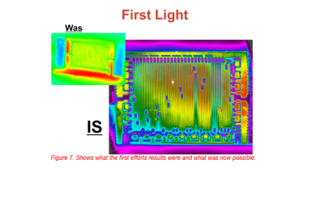
From the first light of the new system it was apparent that there was an improvement and detail once hoped for was obtainable, warts and all. See figure 6 and 7.
FOCUS
The image is not in complete focus because the resistor was not normal to the lens, but it was now possible to see both hot spots and variations in temperatures between the background material and the nichrome film resistive element. With a little more effort and less need for haste the focus was fixed within minutes. Shallow depth of field results in poor focusing ability; the object needs to be normal to the lens, as was already known.
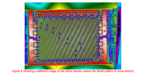
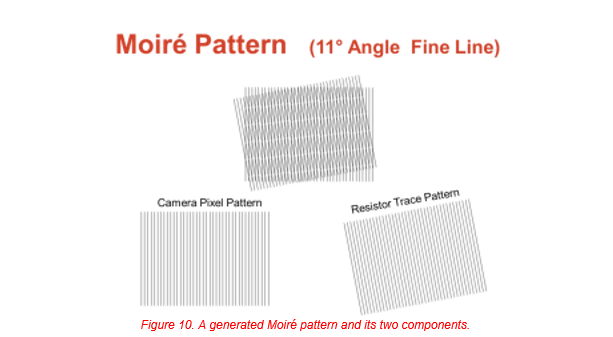
MOIRÉ PATTERNS
While setting up the resistor for the first round of testing Moiré patterns were seen and noted as parallel stripes (See figure 5). With the new setup the patterns were even more apparent. The patterns can be seen in figures 8 and 9. The degree to which they are seen is a function of the angle between the traces in the resistor and the pixels in the camera’s sensor, and the fact that the resistor traces are close in size to the pixels’ size in the camera. The same Moiré patterns can be generated by drawing two sets of parallel lines and overlapping them into one image. See figure 10.
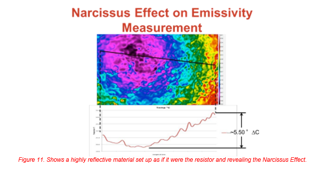
NARCISSUS EFFECT
One of the many settings required to get a temperature reading out of the system is the background temperature. The background temperature (s) are reflected off of the object and into the camera as part of the overall signal. Again nothing new here, but what was a surprise was the entire image was reflecting the inside of the camera, and the camera in use had a cold detector, and not a warm detector. In addition the internal temperatures we could see varied by about 5.5 °C. (See Figure 11.) The background temperature is still needed, but it now needs to be mixed in with the camera’s internal temperature.
EMISSIVITY
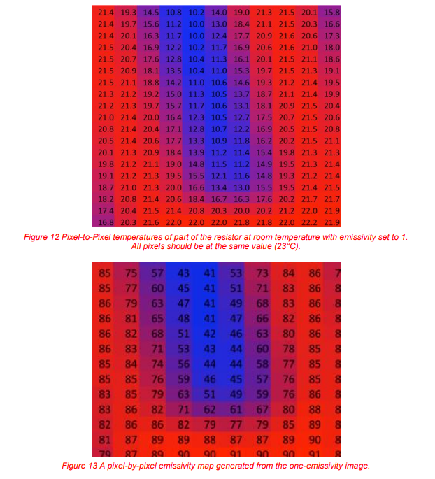
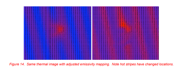
The materials that are seen in the resistor images are nichrome and alumina, with the nichrome being the heating source and the alumina being the heatsink. But the nichrome appears to have a very low emissivity ~0.3 and the alumina has a high emissivity ~0.9 – 0.95. Because of the difference in emissivity and the use of only one emissivity correction factor in the software it makes the alumina appear to be the heat source and the nichrome the heatsink. With only the one emissivity there is no way around the problem. (See Figure 12) If a low emissivity is chosen the nichrome gives a better temperature value, but the alumina appears even hotter (not actually possible). To get a better thermal image it was necessary to manually build an emissivity map one pixel at a time. (See Figure 13) This was possible because the resistor was isothermal at the beginning of the run. In turn it was possible to develop a thermal map using the emissivity map. (See Figure14.)
DUST
For the single emissivity mapped image, dust and marking inks represent a different variation of the emissivity issue. Dust and marking inks tend to have a high emissivity and thus appear to be hotter than their surroundings even when they are heatsinks.
RESOLUTION
The resistor that was used through this test had a known defect. It was easily seen using a SEM. The SEM uses electrons as its light source and they have a very short wavelength and as such have the ability to see very small detail. (In many ways the gold standard for microscopes.) Each microscope, including the SEM, is limited in what it can resolve, and also limited by the wavelength. The resolution is defined by the equation,

Where:
r = Resolution
λ = Wavelength
n= index of refraction of the media surrounding the radiating points
θ = Viewing angle from Normal.
The implication of this is that as the wavelength increases the object being resolved must get bigger.
While mathematically correct its graphical form is difficult to produce and leaves a gray area as to what the limit is and what happens as one gets closer to the physical limit. For a more elegant solution we need to go back to the experiments Isaac Newton (1642 - 1727) did on light and the studies of Jean Baptiste Joseph Fourier (1768 – 1830). Newton did a lot of work on the “composition” of light both white light and colored light. Through his work he was able to demonstrate that by passing white light through a prism it could be separated into its components and then by passing it through a second prism he could reconstruct the white light. He also took one of the individual colors and tried to separate it into its components, and found that once separated it could not be separated further, but by re-combining several colors (not all) he could get different colors, which are a part of white light.
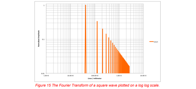
Fourier, while he was originally working with heat and temperature, developed a math that was able to transform dimensions into the summation of a series of sine waves (or look at something in a different way) and in this case we can work between time and space. Newton’s work with prisms is the physical equivalent of Fourier’s mathematical transforms for light. Now it is possible to transform resolution (lines per µm) into wavelengths (frequency or sine waves) and the other way around. It is also possible to digitally remove frequencies and see the effect on resolution.
Resolution is measured in lines per unit distance and uses a target made up of black and white patterns, or for a math model a series of 1’s and 0’s of varying lengths which could also be seen as a square wave. When a Fourier Transform is run (a Fast Fourier Transform (FFT) in this case) the square wave results in
a series that looks like a picket fence with the smaller pickets being at higher frequencies. (See figure 15.) Between the sensitivity of the detector and the frequencies the lens transmit, the shorter wavelengths are lost.
For thermal imaging of large things this is not a loss, and it is what allows the cameras to detect the desired wavelength. But when small things are imaged the shorter wavelengths get closer to the prime wavelength. Figure 16 shows what the removal of the harmonic frequencies does to the square wave. Once the fundamental frequency is lost there is no signal to be seen.

CONCLUSIONS
This paper identified a method for finding defects in small parts, with an emphasis on problems found when using thermal imaging and a microscope. Items from elementary physics include but are not limited to:
- Focusing difficulties when using a microscope.
- Moiré Patterns will show up.
- Narcissus Effects are every present and reflections may not be what is expected. 4. Different emissivity’s needed to be accounted for or distortions will occur.
- The wavelength being detected plays a major roll in what can be resolved.